
 Product
 Brand
Brand
 Articles
 Tools
Tools
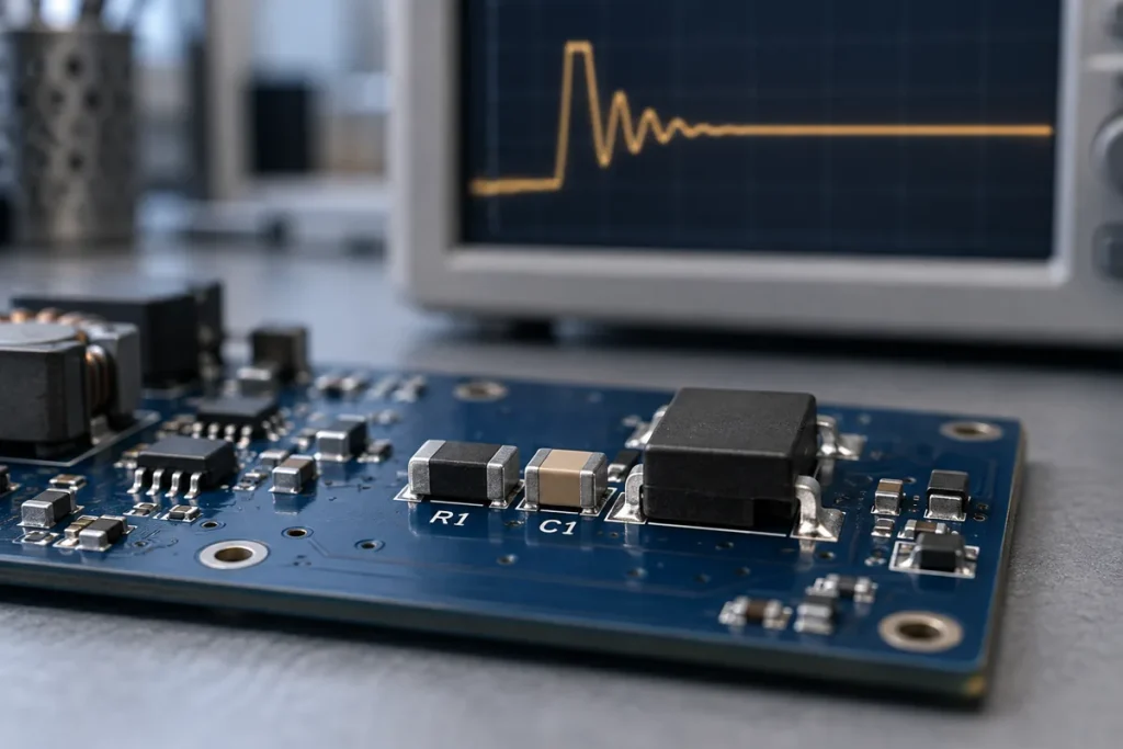
*This is a reference circuit description based on the conventional RC snubber topology used in switching power supplies, as described in the general application guidance that power semiconductor and passive manufacturers publish. It is not a manufacturer’s official reference design and it is not a tested build. Confirm values against the datasheet for the exact switch and against your own measurements.*
The problem the circuit solves. When a switch turns off, the energy stored in the parasitic inductance of the layout is released into the parasitic capacitance of the node. The result is a damped oscillation at the node, typically in the tens of megahertz for a small board. That ringing appears in the switch’s voltage waveform and, more importantly, in the near field around the switch loop, which is why it shows up in radiated emissions measurements at a specific frequency.
The circuit. A capacitor and a resistor in series, connected from the switching node to the power ground — the same return the input capacitor uses, not signal ground. The capacitor dominates at the ringing frequency and the resistor provides the damping. The snubber does not remove the ringing; it absorbs the energy that would otherwise circulate, converting it to heat in the resistor.
Starting values, and why they are only a starting point. The conventional method measures the ringing frequency with the snubber removed. The parasitic inductance and capacitance of the node can then be estimated from that frequency and the known circuit conditions, and the starting snubber capacitor is chosen a few times larger than the node capacitance, with the resistor set to the characteristic impedance of the resulting loop. These are estimates: the layout parasitics are not known accurately, so the values are a starting point for measurement, not a final answer.
Sizing by measurement, not by formula. Fit the starting values, then look at the node waveform with a probe whose ground lead is short — a long ground lead will show ringing that the circuit does not have. Increase the snubber resistor until the ringing is acceptably damped, then increase the capacitor if the damping is insufficient at the lowest practical resistance. Stop when the waveform is clean: every further increase adds loss without benefit.
The cost, stated honestly. The snubber dissipates power continuously, because the capacitor charges and discharges through the resistor on every switching cycle. The loss rises with the switching frequency, with the square of the voltage swing and with the capacitance. At high frequency the snubber can become a significant fraction of the converter’s total loss, which is why an oversized snubber is a real efficiency problem rather than a conservative choice. The resistor must be rated for that dissipation at the ambient inside the enclosure, and its package must tolerate the pulse energy, not just the average power.
Where a snubber is the wrong tool. If the ringing is caused by a switch loop that is far larger than it needs to be, the effective fix is the layout, and a snubber will be treating the symptom at a continuous efficiency cost. If the noise is common-mode and travelling out on a cable, a snubber at the switch node will not address it. And if the switch is already at its voltage rating, damping the overshoot is a reliability measure rather than an emissions one, and the switch rating is the real constraint.
Layout of the snubber itself. The snubber loop is a high di/dt loop in its own right. Its capacitor and resistor belong physically adjacent to the switch and to the power ground, with the shortest possible connections; a snubber placed across the board from the switch node has enough stray inductance of its own to be ineffective at the frequency it was chosen for.
What to verify. The node waveform with a properly short probing ground, before and after. The resistor’s temperature rise at the worst-case ambient, measured rather than calculated. The effect on efficiency at full load. And the ringing frequency against the emissions limit you are actually trying to meet, because damping a frequency that is not the failing one wastes the loss for nothing.
This reference circuit describes a conventional snubber topology and a measurement-driven sizing method. It is not a manufacturer’s reference design and has not been built or measured as part of this article. Confirm component ratings against the datasheets for the exact parts and validate the result with your own measurements.
Specifying snubber and power components?
Send the part numbers and quantities through our RFQ form, or contact us and we will confirm availability and lead time. Our catalogue lists power components and capacitors by category.
—