

 Product
 Brand
Brand
 Articles
 Tools
Tools
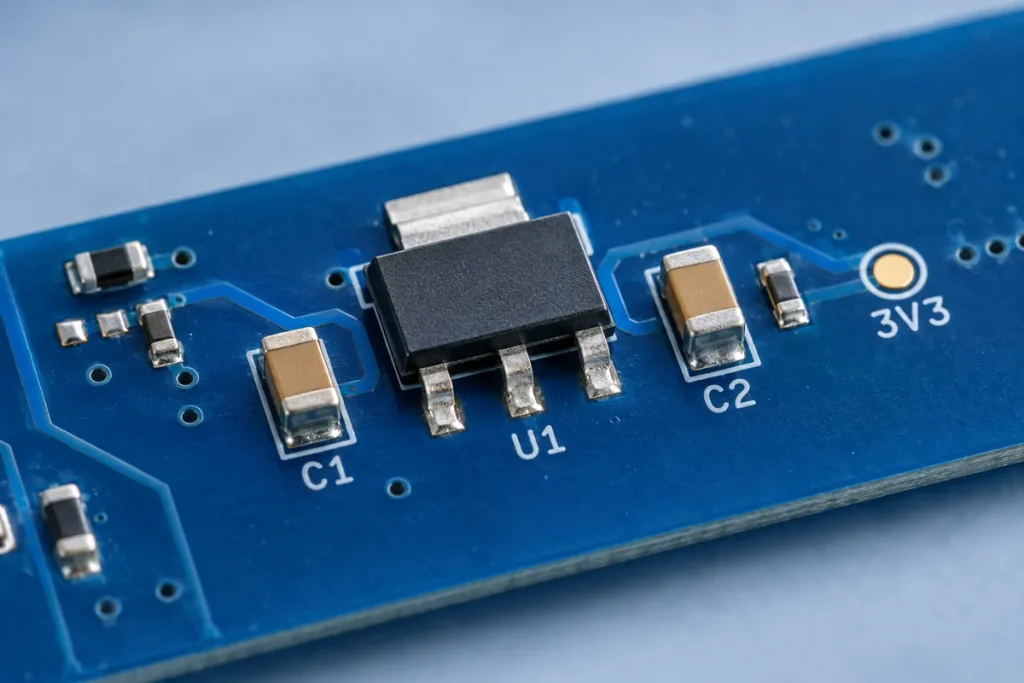
*This is a reference circuit description based on the conventional linear-regulator topology that regulator manufacturers publish in their general application guidance. It is not a manufacturer’s official reference design and it is not a tested build. Confirm every value against the datasheet for the exact regulator you use.*
The circuit. A three-terminal fixed 3.3 V linear regulator in a surface-mount package, with an input capacitor, an output capacitor, and an optional noise-reduction capacitor on the reference pin where the device provides one. The block diagram is unremarkable; the design work is in the values and in the thermal calculation.
Why a linear stage is still the right answer. A linear regulator’s advantage is not efficiency, it is quietness. It has no switching node, so it produces no switching ripple and no radiated field from a switch loop. Where an analog rail or a low-jitter clock supply follows a switching converter, a linear post-regulator is the conventional way to clean it up. The cost is that the regulator dissipates the difference between input and output as heat, which sets a hard limit on the current it can supply.
Input capacitor. The input capacitor’s job is to supply the transient current the regulator draws and to keep the input impedance low at the frequencies where the regulator’s loop gain is falling. Its value is less critical than its placement and its ESR: a ceramic close to the input pin, with a short return, does more than a larger part further away. Where the input arrives over a cable, a bulk capacitor at the connector complements the ceramic at the pin, because the two cover different frequency ranges.
Output capacitor, and the stability trap. Linear regulators of this type are usually specified with a minimum output capacitance and, for older families, a required ESR range. Both matter. Modern ceramic-output regulators are stable with a small ceramic; some older types oscillate with a very low ESR and need a defined series resistance. The correct value is whatever the specific device’s datasheet states, and it is the single most common reason an otherwise correct linear stage is unstable.
Noise reduction and reference bypass. Where the device exposes a reference or noise-reduction pin, a capacitor there lowers the noise contribution of the internal reference. Its value is given in the datasheet and is usually small; making it much larger slows the startup. This is a case where the datasheet value is the answer and there is nothing to gain by deviating.
The thermal calculation, and why it decides the design. Power dissipated is the input-to-output voltage difference multiplied by the load current, plus a small quiescent term. The junction temperature is the ambient temperature plus that dissipation multiplied by the junction-to-ambient thermal resistance, which is a property of the package and the copper area it is soldered to — not of the package alone. The copper area is therefore a design parameter, and a design that passes on a bench with a large plane can fail inside a small enclosure with a reduced pour. Where the number does not close, the options are a lower input voltage, a series resistor ahead of the regulator, a larger package, or a switching pre-regulator — not a larger heatsink on a surface-mount part.
Layout. Input and output capacitors as close to their pins as the layout allows, with their ground returns to the same copper the regulator’s ground pin uses. The output sense point taken at the output capacitor rather than downstream. The heat-spreading copper sized from the thermal calculation and connected to the ground plane with a via array where the package expects it. And no long trace between the regulator and the load it supplies, because the trace inductance is in series with the loop the output capacitor is trying to hold.
What to verify. Output capacitance and ESR against the device’s stability requirement. Dissipation and junction temperature at the maximum ambient the product will see, using the actual copper area. Dropout voltage at the minimum input and the maximum load, since a linear stage that is fine at nominal input can fall out of regulation at the low end. And startup behaviour into the real load capacitance.
This reference circuit describes a conventional topology and the role of each element. It is not a manufacturer’s reference design and has not been built or measured as part of this article. Confirm all values, the stability requirement and the thermal data against the datasheet and the application notes for the exact regulator.
Selecting a regulator stage?
Send the part numbers and quantities through our RFQ form, or contact us and we will confirm availability and lead time. Our catalogue lists regulators by category and package.
—